Diagnosis Solution
Our solution is a solution that diagnoses, analyzes, and stores defects that can occur during semiconductor manufacturing process in real time, and allows users to directly check
data in real time in a closed FAB environment. Furthermore, we pursue a solution that improves the productivity and competitiveness of our customers by lowering the defect rate
and increasing the semiconductor yield by developing a diagnosis solution based on the data analysis obtained through our solution and predicting the problem occurrence.
Accuracy
freqAI
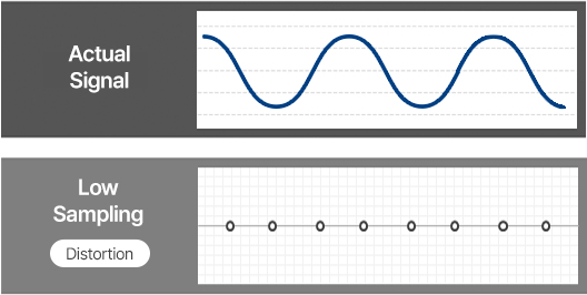
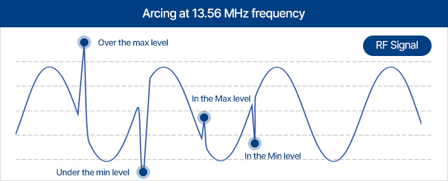
RF sensors are installed on the power transmission line and the frequency signals are analyzed at high speed. The problems of the existing Arcing diagnosis
solution have been improved. WGS’s self-developed ultra-high-speed diagnosis solution.
-
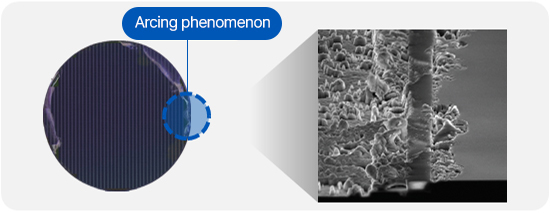 arcing occurs when
- 1. The circuit on the wafer is damaged
- 2. Rework Process, or
- 3. Loss
-
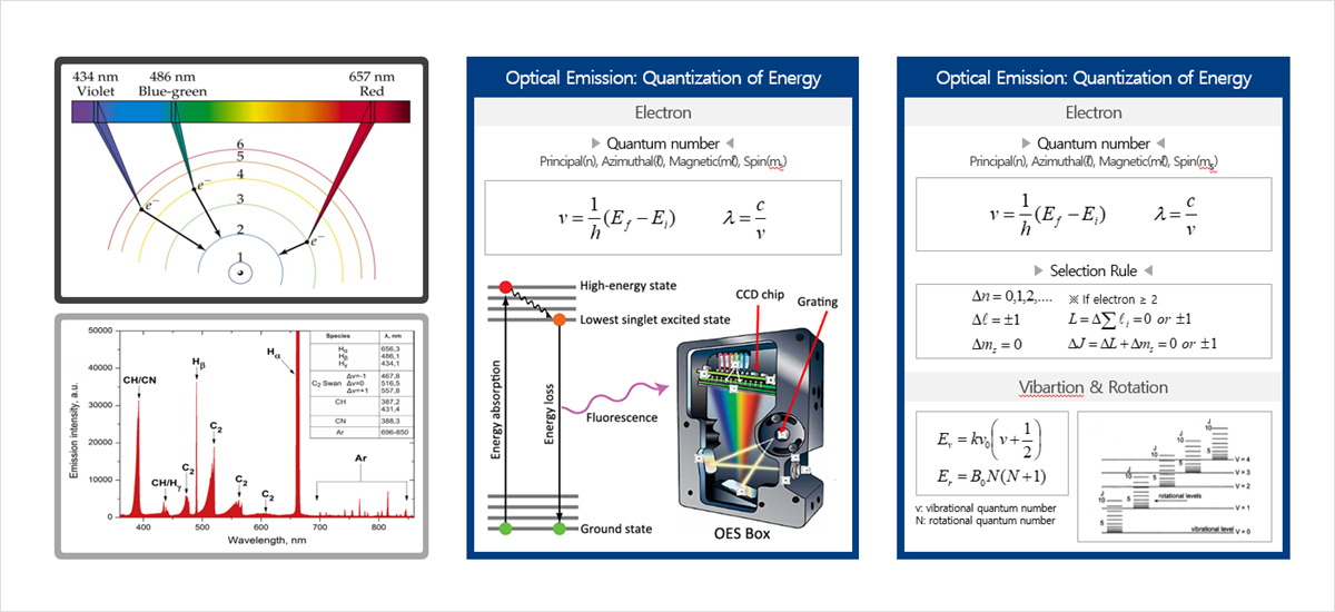
OES System
Optical sensors are installed at the plasma generation location to analyze the plasma formation state. The key to semiconductor yield is “plasma”. Using
OES according to the needs, infinitely expandable diagnosis solution in the process using plasma
